
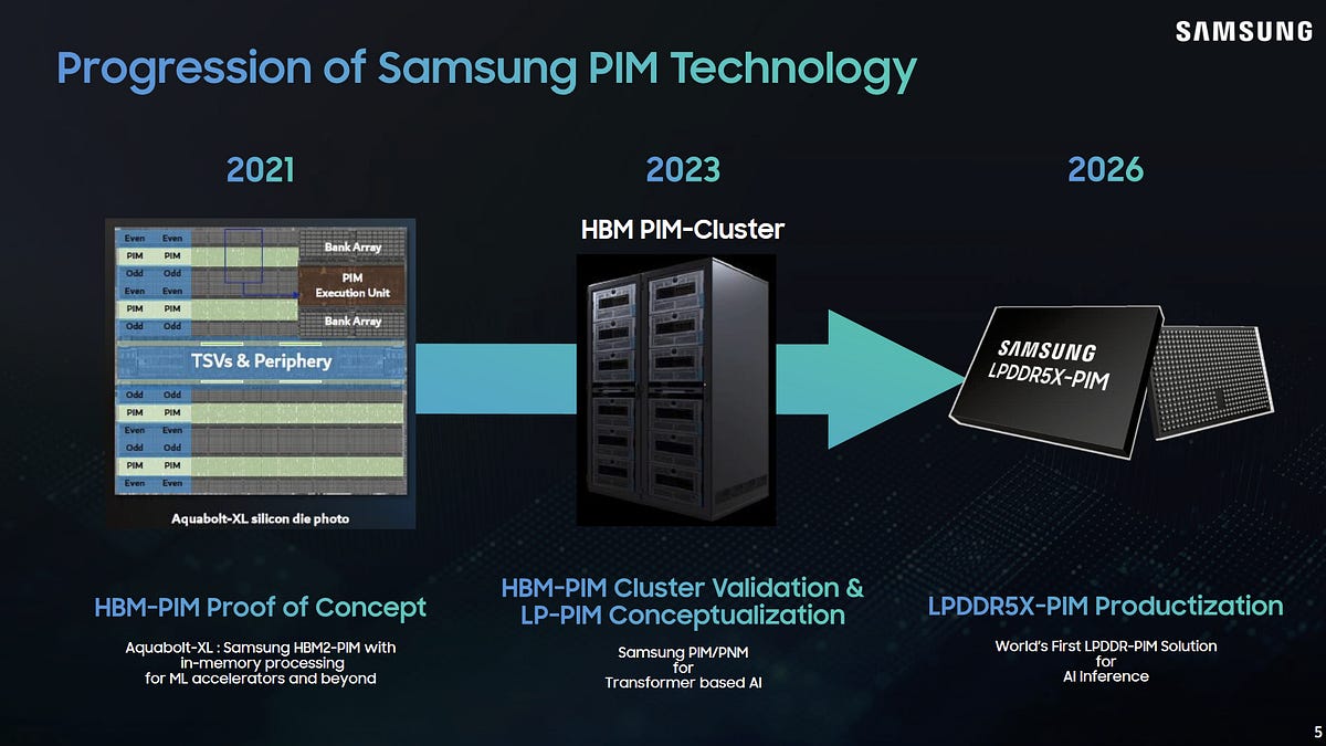
In-memory compute exploits higher internal bandwidth within memory chips, avoiding long latency between DRAM and traditional compute cores. At Hot Chips 2026, Samsung detailed their LPDDR5X-PIM implementation, placing Processing-in-Memory blocks at each of 16 banks in LPDDR5X chips while preserving standard memory controller compatibility. Each PIM block contains a MAC tree with register files and control logic, accessing DRAM banks without being constrained by the external bus.
Together, all 16 banks achieve 614 GB/s internal bandwidth versus 76.8 GB/s for regular DRAM accessing two banks in parallel. The MAC array sustains four INT8 or FP8 operations per data clock, reaching 2.4 TOPS package-wide. Eight LPDDR5X chips would yield 9.6 INT8 TOPS, comparable to Intel's Meteor Lake NPU.
Samsung maintains standard LPDDR5X protocol using special row addresses acting as MMIO controls. Single-bank mode operates normally, while multi-bank mode broadcasts commands across all 16 banks. PIM Registers Activated mode redirects read/write commands to PIM registers instead of DRAM.
Software loads model weights in single-bank mode, then switches to multi-bank mode to write activation values into PIM source registers, set scale factors, and specify operations via instruction registers. This creates a constrained SIMD processor within memory.
Source: Hacker News · Summarized by HeadlinesBriefing